Mini, micro, nano. Things are getting smaller all the time.
Here are some things you can relate to:
-
A credit card is about .020" thick (twenty thousandths of an inch or " 20 mils")
-
A human hair or a sheet of paper is about .005" thick (five thousandths or 5 mils)
-
Aluminum foil in your kitchen is about .001" thick (one thousandth or 1 mil)
These dimensions are not small enough to describe what's happening in the world of electronics. For that, we need to go metric, and then some. A meter is 40 inches. A millimeter is .040" (forty thousandths). A micron (or micrometer) is 40 millionths of an inch. And a nanometer is 40 billionths of an inch.
When I was in high school, the smallest semiconductor transistor (the basic building block of electronics) was 10,000 nanometers. Today, the transistors on the chips in our cell phones are about 20 nanometers. Within a couple of years, they expect that size to drop to about 10 nanometers. And last year, some researchers in Australia created a transistor that is only 0.1 nanometers.
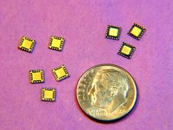
The CPU chips in most of our computers and tablets are about 1 inch square and contain over a billion transistors etched in silicon. Which is all well and good, but how do you connect these tiny things to the outside world?
Metal stamping can't achieve the feature resolution needed. Thus, photo etching is playing a much bigger role in microelectronics packaging. And, the needs being driven by the shrinking size of semiconductor features is pushing etching technology further.
I contacted Richard Sayer of International Phototool Company LLC and asked him about the state of the art in phototooling. His comments are very informative:
"With polyester film, the smallest image sizes that we could achieve on a production basis was about 8 microns on linear features, and 5 to 6 microns on a best-efforts engineering-mode basis. With respect to round/square/hexagonal features, this technology allowed for about 10 micron diameter pads. These dimensions were achievable only the Barco Silverwriter laser photoplotter with souped-up Eagle Optics, plotting at 65,000 dpi resolution. Otherwise, the best available capabilities in commercial production at 40,000 dpi resolution yields feature sizes in the 10 micron (0.0004) range on linear patterns and 15 microns (0.0006) on round/square/hexagonal pads. We only offer imaging up to 40K dpi resolution at this time.
With respect to chrome or iron oxide on glass, we are nowadays able to produce direct-write laser photomasks with linear and round feature sizes down to 3 microns and smaller, with 6-sigma tolerances at +/- 10% of the CD (critical dimension) size. Actually, weve been able to supply these for quite some time, but new technology brought to market within the past few months has allowed us the luxury of rapid throughput (hours vs. days) and much lower prices. Of course, we still produce photomasks with much larger feature sizes, but the low cost and rapid throughput of photomasks with smaller images has allowed for somewhat of an explosion of activity in the areas of MEMS and Microfluidics research and production. Standard mask sizes from 2.5 to 7 square, as well as large area photomasks from 300, 350, 400, & 450 mm square, with custom sizes up to 24 x 28 are now more readily available and with lower prices than ever before.