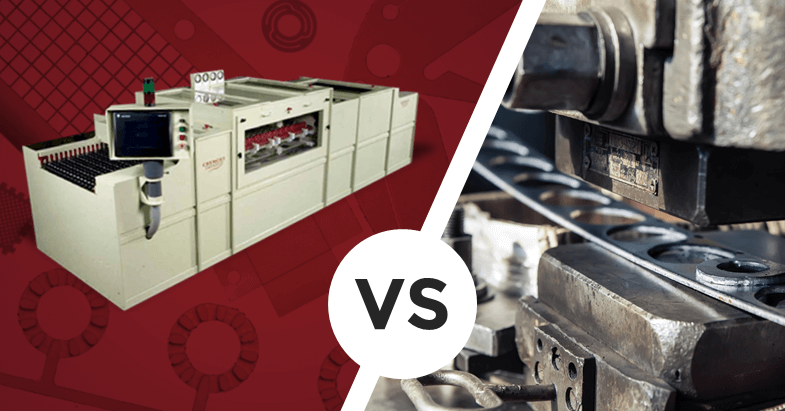
How did you ever survive before photo etching?
We've seen it time and again. From never heard of it to can't manage without it. Photo etching becomes the go-to solution for precision metal parts fabricating once people understand its advantages. Among the key features are inexpensive, rapidly produced phototools ( 1 day), the ability to process metal foils as thin as .0005 inches (really!), and completely "stress free machining": no burrs and no mechanical or thermal effects.
One of the things that adopters of the etching process quickly realize is that complex geometries of parts become non-issues. Whatever the size, shape, number of holes or other types of features are necessary for the function of the part, it's all easy and essentially free. The cost of photo etching is driven by the "real estate": the physical area of the part and the dimensional tolerances, which drive the sheet size. For metals up to .032" thick, drawing block tolerances of +/-.005" allow processing sheets up to 18" x 24", the most economical format, because the unit of labor is sheets per hour. The labor per sheet varies little because 2 hands have to handle whatever size sheet through six distinct manufacturing operations.
So, the economic objective is to get as many parts as possible per sheet. We have put together a table that illustrates the impact of dimensional tolerances and sheet sizes on part costs here. The benefit of understanding this relationship is readily apparent.
Modern design platforms have many manufacturing options "baked in." Stamping, laser, EDM, CNC punching: click a drop-down menu and design rules are applied and cycle times are calculated. But, even when etching would be an absolutely superior option in both cost and quality, designers and engineers have no access to that information.
Part of our mission is to seek out and educate people involved in the design and development of precision metal components about the capabilities of the photo chemical etching process. To get the "30 thousand foot view", this three-minute video about etching will put the right set of pictures in your head. And for more in-depth information, the Comprehensive Guide to Photochemical Machining offers detailed design and process information. (Go ahead...it's free!)
We see photo etching applications in many industries. Electronics and semiconductor packaging; RF and microwave communications; industrial, medical and scientific instrumentation; metal filtration; brazing preforms; aerospace and defense...the list is both endless and changing daily.
So, if you have a fabricated metal application that is just not a great fit for the processes you know, give us a try. We might be exactly what you didn't know you were looking for.
You can reach me at 860-659-0591 or kstillman@conardcorp.com


