Photo etching enables the creation of complex precision parts while keeping production times and costs low.
Engineers and designers at OEMs are often tasked with creating startlingly complex parts while keeping costs and time to market down to a minimum.
For fabricating simple product geometries, photo etching is certainly a smart choice, but the difference between it and other methods may not be as pronounced. However, as these designs become more complex, photo etching's unique advantages offer substantial benefits in cost and precision.
Why does photo etching lend itself so well to complex applications?
Photo etching has proven to be superior to other methods both conventional and nonconventional when it comes to producing complicated products with a high degree of precision.
In photo etching, the part is machined all at once because the process etches through all unmasked areas of the plate simultaneously. Other methods like CNC punching, laser cutting and wire EDMs work on a small, localized area of the part at one time. These methods take more time than photo etching, are highly vulnerable to undesirable effects like tool wear, uneven locational tolerances and thermal and/or mechanical distortions that lead to deficiencies in the final product.
OEMs take notice of photo etching's capabilities
Dr. David M. Allen, a professor of micro engineering at Cranfield University in England, wrote that photo etching has drawn the eyes of engineers and designers in the microelectronics, mechanical and electrical industries over the last half-century for its ability to provide quick response service for complex precision parts.
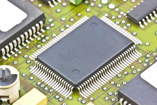
OEMs in these verticals have a high demand for thin gauge (< 2mm in thickness) precision component parts of varying complexity at as low a price point as possible. Allen found that some of the most common examples of this are integrated circuit leadframes, disk drive suspension head assemblies, sieves and meshes, washers, laminations and etched gaskets for use in mobile phones.
Leadframes - a point of comparison between fabrication methods
To test specific examples of photo etching's capacity to deal with complex geometries, the Photo Chemical Machining Institute (PCMI) asked a wide range of companies proficient in different production methods to quote them for parts of various intricacy. Based on the quotes obtained, it was apparent that photo etching was the superior fabrication method as part complexity increased.
One part for which the PCMI received a quote is a leadframe - a part commonly used in electrical circuits. The organization asked a variety of manufacturers to quote them for a 1 inch leadframe made of nickel iron with a thickness of .008" and a dimensional tolerance of +/- .001".
The only method that found it practical to even attempt to make leadframes was laser cutting. The quoted price for tooling and setup for the laser cutting of 100 parts was 270 percent of the price that photo etching could do for the same part. For bulk purchases, it turned out that the cost of manufacturing 5,000 leadframes was also 270 percent of the cost of etching the same size batch. Batches of 50,000 and above were found to be impractical for laser cutters.
Other fabrication methods like stamping, wire EDM and water jet cutting fared even worse. These companies couldn't even quote a price for leadframe manufacture - they all found it to be impractical even in small batches due to the complexity of the part.
Engineers and designers have many options for simple precision parts. But for the more complex products, the capabilities of photo etching can keep production times and costs low.