
Unlocking Innovation: Elevate Your Precision Metal Designs with Photo Etching
Published by
Kathleen Stillman
on
Pushing Design Boundaries
For engineers and designers striving to push the boundaries of precision and complexity in metal component design, finding the right manufacturing method is crucial. Many traditional machining techniques—such as stamping, laser cutting, or wire EDM—come with limitations in terms of cost, material waste, and design flexibility. That’s where Photo Chemical Machining (PCM) comes into play.
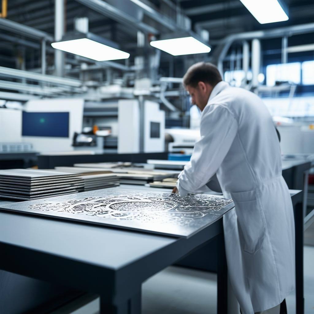
PCM, also known as photochemical etching, is an advanced metal fabrication process that uses light-sensitive materials and chemical reactions to etch precise patterns into metal sheets. Unlike conventional machining, PCM allows for intricate designs without mechanical stress, making it ideal for applications where accuracy, complexity, and material integrity are essential. Let’s explore why engineers and designers should consider integrating PCM into their manufacturing toolkit.
-
Unparalleled Design Freedom and Free Complexity
A disk, a washer and a screen are all the same thing in photo etching, all that matters to cost is the “real estate,” and the tolerance band.
One of the most significant advantages of PCM is its ability to create complex geometries and intricate patterns that would be nearly impossible or prohibitively expensive with other methods. This process allows for:
- Fine details and tight tolerances—PCM can achieve tolerances as low as ±10% of metal thickness, making it perfect for delicate or high-precision components.
- There may be cost implications that can be reduced with more generous tolerances.
- Burr-free edges—Unlike stamping or laser cutting, which can leave rough or heat-affected edges, PCM produces clean, burr-free components that require little to no finishing.
- Micro features and high-density patterns—PCM can create features as small as 100 microns, enabling the development of fine meshes, microfluidic devices, and intricate aerospace components.
-
Material Versatility for Diverse Applications
Another key benefit of PCM is its ability to process a wide range of metals, including:
- Stainless steel (commonly used in medical and aerospace industries)
- Aluminum (lightweight and corrosion-resistant, perfect for automotive and aerospace components)
- Copper and brass (ideal for electronics and heat exchangers)
- High Nickel alloys including Inconel, Kovar, Alloy 42 and others (used in high-performance applications where strength and durability are paramount)
Unlike other processes that struggle with hard-to-machine materials, PCM maintains the integrity of these metals without introducing mechanical stress, ensuring superior performance in demanding environments.
-
Cost-Effectiveness for Prototyping and Production
When developing prototypes or small production runs, traditional tooling and machining methods can be expensive and time-consuming. PCM eliminates the need for costly hard tooling, offering:
- Lower initial costs—No expensive dies or molds are required, making it more affordable for low to mid-volume production.
- Quick turnaround times—Because PCM relies on photoresist and chemical etching rather than mechanical tooling, designs can be quickly modified and produced, reducing lead times.
- Scalability—While PCM is excellent for prototyping, it’s also highly scalable for full production runs, offering a smooth transition from design iteration to mass manufacturing.
-
Minimal Waste and Environmental Benefits
Sustainability is an increasing priority for engineers and designers, and PCM offers several eco-friendly advantages:
- Reduced material waste—Unlike machining or stamping, which can produce significant scrap material, PCM removes only the necessary areas, maximizing material utilization.
- No mechanical stress or heat distortion—Since the process doesn’t use force or extreme heat, there’s no warping or material weakening, preserving the original properties of the metal.
- Recyclable chemicals—Many etchants used in PCM can be recovered and reused, reducing the overall environmental impact of the process.
-
Wide Range of Applications Across Industries
PCM is widely used across various industries that require high precision, lightweight, and intricate metal components. Some common applications include:
- Aerospace—Lightweight, high-strength parts such as turbine components, fuel filters, and heat exchangers.
- Medical Devices—Surgical instruments, implantable medical components, and microfluidic devices.
- Electronics—EMI/RFI shielding, lead frames, circuit boards, and precision contacts.
- Automotive—Fuel injection nozzles, heat exchanger plates, and fine filtration components.
- Consumer Electronics— Cell phones, TVs, Tablets and more
-
Final Thoughts: The Future of Precision Metal Fabrication
As engineers and designers continue to develop more intricate and high-performance metal parts, the demand for advanced fabrication methods like Photo Chemical Machining will only grow. Whether you’re looking to create ultra-precise aerospace components, innovative medical devices, or complex electronic circuits, PCM provides a cost-effective, high-precision, and environmentally friendly alternative to traditional machining.
By embracing PCM, you can expand your design possibilities, reduce costs, and improve efficiency—all while maintaining the highest standards of quality. If you haven’t yet explored the potential of Photo Chemical Machining, now is the perfect time to incorporate this game-changing technology into your design and engineering process.
Request A Free Quote Today
Tags:
Photo chemical etching,
Aluminum Photo Etching,
Metal Filtration,
metal etching,
Cost of Photo Etching,
DFM,
Dimensional tolerances