
Precision Metal Fabricating without Stress
Photo etching is a "non-conventional" method that fits alongside stamping, punching, laser, and wire EDM for manufacturing many types of metal parts. Suited to many metal alloys, etching eliminates problems common to other processes: burrs and cold working in stamping and punching, heat affected zones or recast layers for laser and wire EDM. It is particularly capable with very thin materials (routinely down to .001") and both reflective and thermally conductive metals such as aluminum and copper.
Here's a quick run down of etching specs and tolerances.
For more detail:
Chemical machining or etching is a method of fabricating metal components that relies on an acidic solution to dissolve unwanted metal. The photo etching process is used for fabricating metal parts for many different industrial applications including sensors, shields, retainers, flat springs, strain gauges, filters, screens, grids, shims, gaskets and more. For electronics, etching is used to produce a host of metal components used in RF, microwave and wireless applications, as well as lids and leadframes for microelectronics packaging. Photo etched direct bond copper is increasingly used in power electronic applications, particularly in wireless devices. It is also used to produce a host of electrical contacts, buss bars and other electrical interconnect devices.
Get the picture here : 3-minute video shows the processPhotochemical machining can be a very economical alternative to stamping, laser or EDM. With inexpensive film-based tooling that can be produced in a day, rapid prototyping is easily achieved. Order minimums are modest and can produce dozens to hundreds of parts at low cost.
To help engineers and designers in their design-for-manufacture (DFM) decisions, we have published a basic DIY Guide to Estimating Photo Etching Costs. It's Free!

From Data to Details
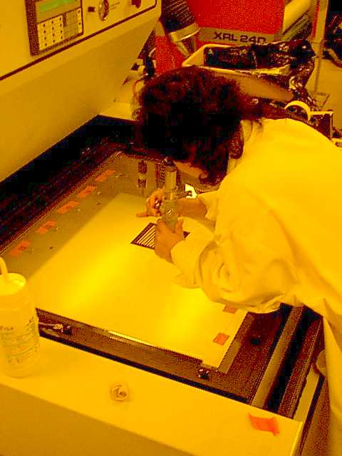
The basics of the process include creating the photomask, which today is derived from CAD data and output on film from a laser photoplotter. This is known as the phototool. The metal to be etched is carefully cleaned and coated on both sides with a polymer film called photo resist. When applied, the photoresist film is unexposed and this must be done in a yellow safe-light environment.

The coated metal and the phototool come together in the imaging process where the black regions on the phototool prevent the exposure of the resist under intense UV light. The unexposed resist is washed away in a developing solution, leaving bare metal in the areas to be etched.
In the etching process, the exposed photoresist is strong enough to withstand the effects of the ferric chloride etchant. But the unprotected metal is dissolved right up to the edge of the resist. The etchant is sprayed at both sides of the sheet until cut through is achieved. After etching, the resist is washed away in a different solution.
Photo Etching vs. "the Others"
Photo etching is also known as chemical etching and photo chemical machining. It evolved in the 1950s as an off-shoot of printed circuit board fabrication, and the production process is very similar.
Stamping and punching utilize hardened steel tools to shape metal parts. Plasma, laser and water jet cutting utilize directed energy to shape parts. And, wire EDM uses a wire electrode to burn away metal.
So, just by thinking about the processes, you can easily see the differences. Stamping and punching are sort of "brute force" processes, shearing the metal using powerful presses. Plasma, laser and EDM rely on intense energy, literally burning their way through metal. Waterjet is sort of the "hot knife through butter" option, but you definitely wouldn't want to get in the way of a pressurized stream of water that can cut through an inch of steel!
Photo etching, in contrast, would be like running a sheet of metal through your dishwasher and then taking out a sheet of parts.
Applications for Every Occasion
So, what can you do you with photochemical machining? You can make very thin metal parts, as thin as .0005" (yes, five ten-thousandths). You can make fairly thick parts: up to .040" in ferrous alloys, .065" in copper alloys, and .080" in aluminum. You can make parts with funny shapes and lots of holes and it doesn't cost any extra. You can make some very little parts, as small as .020" diameter. And, you can make some fairly big parts, up to 24" x 60".
Do you have a project in mind?

ADDITIONAL RESOURCES

The Comprehensive Guide to Chemical Machining
DOWNLOAD

Introduction to Electroforming


Design Considerations for Photo Etching
DOWNLOAD