Photo etching is the process of choice for fabricating metal components used in an impressive range of industrial applications, both mechanical and electrical/electronic.
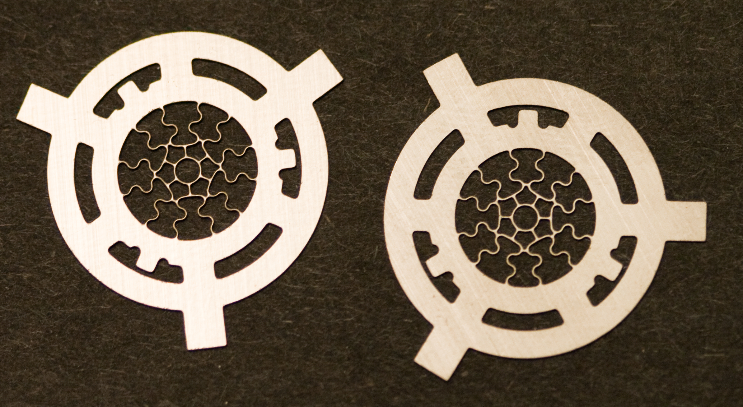
Manufacturers of scientific and medical instruments, such as blood and gas analyzers, spectrometers, seismographic devices, metrology instruments, MRI equipment and many more utilize photo etched parts. For power generation/storage devices, including turbines, fuel cells and batteries, chemical machining is the only practical process for manufacturing parts with complex structures.
Even simple parts, like shims and spacers, can be readily and economically produced in a range of materials and thicknesses. Etching is also convenient for flat springs, shields and retainers.
Find more detail about mechanical applications here.
Filtration, from finely detailed deposition masks to robust separation screens in food processing, is another application where metal etching has some meaningful advantages because the incremental cost of holes is "zero." Whether it's one hole or a million, there is no additional cost in the tooling; there is no additional time in manufacturing and no additional cost at all.
On the electronics side, photo etching is the darling of wireless communications. From the handsets to the towers, the "un-wired" world benefits from the ease of fabricating unusual geometries, quickly and cost effectively. And, even at the chip level, high density leadframes can be coaxed into being using high resolution phototools.
Copper alloys, including beryllium copper and phosphor bronze, are readily etched and have great utility in making resilient electrical contacts. Nickel alloys figure prominently in electronic packaging, particularly with regard to the "controlled expansion" classes of nickel-iron (Invar, Alloy 42 etc) and nickel-iron-cobalt (Kovar).
The popular construction for power electronics circuits is direct bond copper (DBC) on alumina or aluminum nitride. The big factor in these devices is shedding heat, which is the main purpose of the ceramic substrates. Photo etching is the only practical fabrication process.
Flexible resistive heating elements and flex circuits are also in the set of electrical applications.
For additional information about design and applications for photo chemical machining: