The umbrella term power electronics refers to a range of semiconductor devices that are used to manage and manipulate the voltage, current and frequency of electric power. 
- If it has a battery, it needs a special semiconductor that maintains the correct operating voltage to the device regardless of the voltage state of the battery.
- If it plugs into the wall, it needs a device to convert and step down the AC to DC.
- If you are charging a battery from an AC source, you need a semiconductor that converts the AC to DC at the correct voltage.
- If you are generating electricity from a variable source such as wind, solar, hydro, you need a semiconductor that converts the fluctuating AC to clean DC and then back to clean AC.
- Uninterruptible power supplies store DC power and output AC power.
Common names for these types of devices include inverters, converters, and rectifiers. It's all about managing and converting flows of alternating (AC) and direct (DC) current.
And, whenever you are dealing with the flow of electric current, you are also dealing with heat. Delicate electronics and heat are not a good combination.
The modern solution is to combine a conductive material, like copper, with a non-conductive material that is also good at dissipating heat. That's where ceramics come in handy. They don't conduct electricity and they are good at dissipating heat.
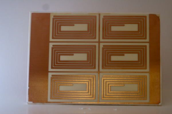
Direct bond copper (DBC) is the go-to solution. Copper foil, usually 5-, 8- or 12-mils thick is diffusion bonded to one or both sides of a ceramic card.
The most widely used ceramic is aluminum oxide, or alumina, which has heat dissipating capacity up to about 48 w/mK (watts per meter*Kelvin.) Aluminum nitride (AlN) can dissipate over 150 w/mK. Aluminum nitride is about 3 times the cost of alumina.
Fabricating the DBC substrates into useful devices relies on photo etching the circuits into the copper. Chemical etching selectively removes the copper without affecting the ceramic in any way. The phototool is designed to replicate as many copies of the DBC circuit as will fit on the tile. The individual circuits are spaced to allow secondary fabricating processes after photo etching.
Additional fabricating steps include laser scribing and, often, hole drilling. The laser scribing allows the ceramic to be cleanly snapped into single circuits. Most often, the etched substrates are plated with electroless nickel and immersion gold, a process known as ENIG. Given the current cost of gold, some users are switching to a three step plating process known as ENEPIG, which places a layer of electroless palladium under the gold to allow the gold weight to be reduced.
The etched, scribed and plated substrates typically will have one or more surface mounted components wire bonded to the gold. After the components are assembled, the individual circuits are singulated and are ready for the next assembly process.
DBC circuits are found in nearly every mobile device and a wide range of wireless communications products. As devices become smaller and more powerful, the need for DBC circuits to manage energy and heat becomes ever more important.
Photo chemical etching is the most cost effective solution for processing copper on ceramic substrates. It produces a crisp, clean circuit free of burrs or distortions. We have extensive experience etching clad substrates products for a wide variety of applications.
If you would like more information, please: