
The booming market for wearables is presenting considerable opportunities for MEMS manufacturers, and photo etching can help.
Consumers are going crazy for wearables - "smart" devices that track personal health and fitness data and present it to the wearer in a way that allows them to make better nutritional and exercise decisions. Recently, Micro Manufacturing looked at research from Gartner and found that the total market size for the wearable products category is slated to reach 91.3 million units shipped by the end of 2016, up from 68.1 million units in 2015.
New wearables call for small size, big performance
OEMs that get tasked with making these devices are going to have their work cut out for them. The thing with wearables is that the products are getting smaller and smaller. And don't think for a second that smaller means less powerful - the companies that put their names on the products want their customers to know that they can get these mini-devices without sacrificing performance.
As Micro Manufacturing wrote, these always-on, always-connected products use a considerable amount of power. This is no small feat when you consider just how small these batteries and other component parts are getting. To maximize the device's potential, OEMs must find the most efficient combination of mechanical and electrical components that can fit all on one miniscule chip substrate. The components we're talking about here involve MEMS accelerometers, sensors, semiconductors and other familiar parts, just brought down to the micro level.
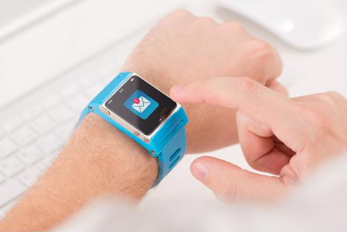
 The market for wearbles is growing, and so are the opportunities for MEMS manufacturers.
Making complex, precision component parts at scale - what Photo Etching does best
As the Gartner report showed, we can expect the market for wearables to explode within the next two years, and it's likely that OEMs in the MEMS space will have ample opportunity to get in on the action.
Manufacturers in this field are already well acquainted with producing parts for the RF & Microwave and wireless industries, which gives them a head start - most of these technologies have already made their way into wearables and other products that fall under the "Internet of Things" umbrella.
"Photo Etching is one of the most effective and efficient ways to take a complex, flat design and turn it into a finished product."
With the high number of units expected to ship by the end of next year, OEMs are going to be expected to produce at a breakneck pace to keep up with demand. This is where things start to get complicated: They will need to create highly functional, complex component parts designed to fit in increasingly small spaces, and they'll need to deliver them in massive batch sizes.
Fortunately, there's a fabrication process that suits this need perfectly: Photo Etching is one of the most effective and efficient ways to take a complex, flat design and turn it into a finished product. In fact, as the Photo Chemical Machining Institute found, the more intricate the part, the more cost effective it is to use Photo Etching as a means of fabrication.
One reason why Photo Etching is great for this type of work is that we can work with thin-gauge metals and hold tolerances within .001" for sheets with a thickness of .005" and under. Additionally, the process produces no burrs or thermal distortions in the finished product. This is absolutely key when making parts where even the slightest flaw can compromise the finished product.
Another thing that makes Photo Etching an excellent choice, especially where big batches are concerned, is that the tooling costs are very low compared to other fabrication methods like stamping, milling and laser cutting. Phototools can be generated in a matter of hours from a customer-supplied CAD file. Most tools range in price from $185 to $350, and can be rapidly and inexpensively regenerated to accommodate revisions to parts.
For more information about the photochemical etching process: 
If you're an OEM who is already involved, or is looking to move into the MEMS space, call us at 800-443-5218 or email us at sales@conardcorp.com and let's get started working on your designs!