
From semiconductors to fuel cells to filtration to medical devices --and many more-- major OEMs, names you will instantly recognize, use photo etched precision metal parts in key applications. Given the vast array of metal fabricating resources and technologies available to leading OEMs, why would they choose photochemical etching for critical elements of their products?
The primary drivers for the photo etching option include:
- It's the best way to produce a given part. Other processes may leave undesirable vestiges or affects on the metal.
- It's the only way to produce a given part. Other processes may be incapable of resolving certain levels of detail, or may be ill-suited to processing very thin materials or certain alloys.
- It's the most economical way to produce a given part. For fine filtration products and many semiconductor packaging devices, among others, photo etching is far more cost effective and produces a superior product compared to other possible solutions.
- It's the best balanced option. Low cost tooling in a day (compared to stamping) and low effective unit costs compared to laser, water jet or wire EDM.
Unfortunately, photo etching is also the least known option in metal fabricating. Educating designers and engineers about the capabilities of photochemical machining (yes, this is the "formal" name) is our biggest job.
Applications where photo etched components are widely used include:
- Fuel cell stacks and flow plates
- Rechargeable batteries
- Heat transfer/exchange devices
- Turbines and bearings
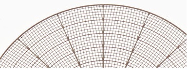
- Filters, screens, grids and meshes
- Analytical instruments for scientific, medical and industrial uses
- RF, microwave and wireless communications
- Mechanical linkages and electrical interconnects
- Microelectronics and power electronics
- Controls, actuators, sensors
- Waveguides, seals, gaskets, shims
- Flexible heating elements and magnetic field coils
Industries utilizing etched metal components include:
- Aerospace & Defense
- Automotive
- Consumer Electronics and Appliances
- Energy
- Food Processing
- Chemical Processing
- Water and Waste Processing
- Medical
- Communications
- Semiconductors and Electronics
- Industrial and Scientific Instruments and Controls
- and many more
The potential applications for PCM are only limited by the relatively small community of people who are familiar with the process. Our goal is to spread the word and share the wealth.
Here's an introduction to Understanding Etching Costs and some information about tolerances
For more technical info: 
To reach me: 800-443-5218 or kstillman@conardcorp.com.