
The accelerating evolution of 3D printing technologies is garnering a lot of headlines. And, while it is likely that these technologies will enable the manufacture of an astounding variety of products, it is also likely that 3D printing will continue to be slow and costly compared to other metal fabricating processes.
Advances in electronics technologies are also accelerating. Just this week, a group of researchers at UC Riverside announced the development of a process to produce anodes for lithium ion batteries from sand. This discovery could increase the charge capacity of these batteries by a factor of three. As electronic devices become smaller, more powerful and more interconnected, the need for increasingly delicate yet robust means of connecting semiconductor chips to their inputs and outputs only grows.
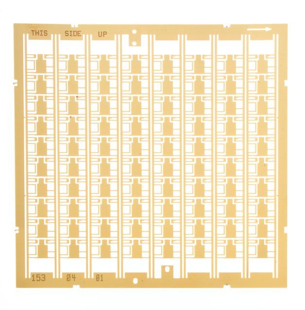
Photo etching accommodates fabricating a wide selection of metal alloys, including many copper- and nickel-based alloys that are widely used in microelectronics packaging devices including leadframes, lids and contacts. The ability to photo etch leadframes and other contact devices in arrays facilitates automated wire bonding of the semiconductor dies.
Smaller, more powerful and power-hungry devices benefit from the dimensional stability and heat dissipation characteristics of direct bond copper on ceramic, usually aluminum oxide, or aluminum nitride for even higher heat dissipation. Photo etching is the only practical solution for creating circuit patterns on DBC substrates. DBCs are usually etched and then laser scribed ( and sometimes drilled) for singulation. Common plating options include electroless nickel, either alone, or with immersion gold. We can provide end-to-end support for these services.
Chemical etching finds a broad swath of uses across the entire spectrum of wireless technologies, with new devices and designs emerging, it seems, daily.
We receive frequent inquiries about etching applications in alternative power; new display technologies; medical, scientific and industrial instruments and sensors; as well as astoundingly long-lived aerospace and defense systems.
Between the newest of the new and the durable legacies, photo etching is a relevant and versatile process for producing precision metal components. After nearly 50 years in this industry, we know we haven't seem it all.
Digitally driven technologies like lasers, waterjets and now 3D printers, are less about replacing other processes and more about expanding the ranges of things that can be done more easily and effectively.
If you have an application you would like us to look at: 
If you would like to learn more about the photo etching process: 
And, if you just want to talk, call me at 800-443-5218.