Photo etching is a powerful option for OEMs looking for a supplier of precision component parts for sensors.
Devices, equipment and consumer products are increasingly equipped with sensors and other communicative technologies. These sensors - and their components - interact mechanically with their environment and electronically with the system or device to which they "report". Here are a few common applications for sensing/measuring technology today:
- Scientific instrumentation - atmospheric sampling, strain gauges, mass spectrography, chromatography, photometry and other lab equipment.
- Industrial machinery - flow and capacity sensors, pressure membranes and electronic traceability.
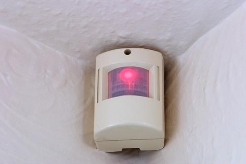
- Consumer goods - kitchen appliances, smart thermostats, automobiles, smoke and carbon monoxide detectors, etc.
Because sensors must be small enough to be noninvasive to the normal functioning of the device, yet still powerful enough to perform at an optimal level, fabrication processes must be able to accommodate very strict design standards. Photo etching is one process that can tackle these difficult manufacturing challenges. Here are some of the key reasons why:
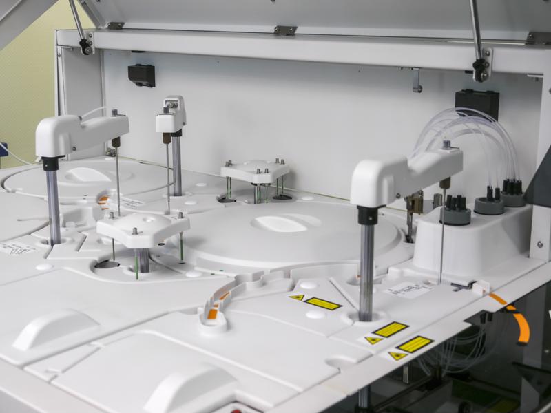 Modern medical and scientific equipment rely heavily on sensors.
Cost-effective at any production volume
Machining complex flat metal parts can get very expensive if you're using conventional processes such as laser cutting, stamping or wire EDM for large production runs. This is mostly because the tooling costs - creating dies for stamping, for example - with these processes increase along with volume. Photo etching doesn't run into that issue because we don't have any "hard" tooling.
Using a CAD file with your part's design, we generate a phototool. This is a stencil in the shape of your finished part printed on dimensionally stable mylar using an 8,000-dpi photoplotter. Since UV light is the phototool's only working exposure, there is no tool wear in the traditional sense of a die or drill getting worn out from multiple uses. The phototool can be created for about $300 or less and be ready within a few hours. Because we're just printing them, phototools can be easily regenerated for multiple production runs without running your costs up.
Part complexity is a non-issue
During the etching process, the phototool is laminated to both sides of a sheet of metal, leaving the metal bare where the part is to be etched. The sheet is exposed to the etching solution (usually ferric chloride), and the exposed metal is dissolved all at once, leaving the final part.
Because the "machining" happens simultaneously, we can create very intricate parts - with odd shapes or lots of holes - quickly, easily and accurately. Conventional processes like CNC punching, laser and EDM can only work on one small localized area of the part at a time. The more complex the part, the more time it takes - another major cost driver.
Dimensional accuracy
For sensors and other microelectronics to work properly, each component and subassembly needs to be precisely made. They have to fit into small spaces, and a part that's even slightly out of tolerance can throw the whole thing off. Photo etching is able to hold tight tolerances, so your parts come out to your specifications without worrying about adverse effects created by conventional processes like thermal and mechanical distortions or burrs. The tolerances we hold depend on the thickness of the metal sheet:
- Minimum dimensional tolerances of +/-.001" are achievable on metals up to .005" thick.
- For metal over .005" thick, minimum dimensional tolerances will be +/- 15% of metal thickness.
- Location tolerances will be within +/-.001" of drawing nominal.
To learn more about photo etching, call us at 800-443-5218 or email us at sales@conardcorp.com and we can get started working on your designs!