
Photo etching has evolved from a niche process to one that serves a wide variety of industries with precision metal fabrication needs.
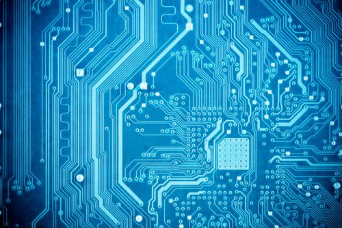
Photo etching, also known as chemical etching and photo chemical machining, has evolved from the printed circuit board industry in the 1950s to nearly every industry that has a need for precision metal fabrication. Despite its many uses the process is not well known to engineers and designers who develop OEM products. If you're unfamiliar with the process, watch this 2-minute video:
As you can see, etching is a unique process. But why should you choose it over other fabrication methods?
How photo etching compares to the conventional processes
Stamping and punching utilize hardened steel tools to shape metal parts. Plasma, laser and water jet cutting direct intense energy to shape parts. Wire EDMs use a wire electrode to burn away metal. Each of these processes rely on "brute force" - shearing, cutting or intense directed energy - which may lead to undesirable effects like heat-affected zones (for the high-temperature processes), mechanical distortions and burrs. For designs that require tight tolerances, these effects can be the difference between a working part and scrap.
By contrast, photo etching uses no hard tooling, and the highest temperature the process reaches is about 135℉ - roughly the same as your dishwasher. It doesn't affect the composition of the metal in any way, so it's exempt from Nadcap checklist 7108/5.
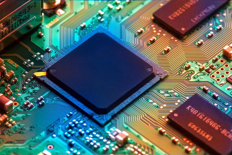 PCM had its start in the printed circuit industry, but has since evolved to take a critical place in a diverse collection of verticals.
Wide Range of Metal Gauges, Alloys and Part Sizes
- Metal thickness ranges from .001" to .080" depending on the type of metal.
- Part sizes from .020" diameter to 24" x 60".
- Metals include steel alloys, copper, aluminum, molybdenum and much more.
- Drawing block tolerances of +/-.005" are achievable on metals up to .032" thick.
- Minimum dimensional tolerances of +/-.001" are achievable on metals up to .005" thick.
- For metal over .005" thick, minimum dimensional tolerances will be +/- 15% of metal thickness.
- Location tolerances will be within +/-.001" of drawing nominal.
OEMs in many industries including microelectronics, medical and scientific instruments, RF & Microwave and aerospace rely on photo etchers for precision parts that are impractical or impossible for other fabrication methods. Mechanical parts include sensors, shields, retainers, flat springs, strain gauges, filters, screens, grids, shims, and gaskets. Electronics applications include contacts, reeds, leadframes, hermetic lids, antennas, and direct bond copper. New applications are emerging every day that photo etching can fulfill in a timely and cost-effective manner.
Our Comprehesive Guide to Photo Etching answers many technical questions for engineers. The download is free! Get The Guide Now
For more information on the etching process, or to see how OEMs can benefit from working with a photo etching provider, call us at 800-443-5218 or email us at sales@conardcorp.com and we can get started working on your designs!